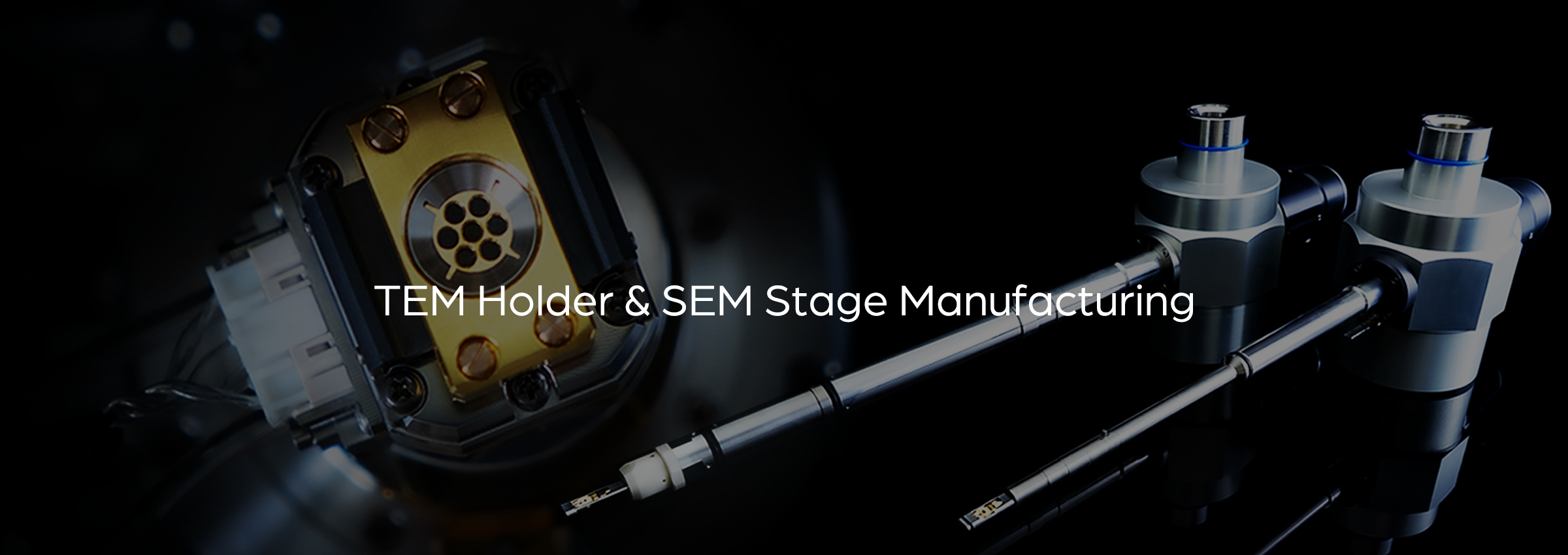
Latest NEWS!! The new addition to the HATA-Holder series, a revolutionary innovation for future much less drift and 360 degrees tomography. Sincerely yours. Mel-Build


  Happy New Year 2012


Note

  Product design or product specifications are subject to change without prior notice.
  FEI, FEI Company, FEI (stylized logo) and Tecnai, Titan are either registered trademarks or trademarks of FEI Company
  Gatan, Gatan Company, DM, Digital Micrograph and USC Camera are either registered trademarks or trademarks of GATAN Company
  Mel-Build products include technology with patent protection and patents pending.
  Mel-Build products are regulated to legislation of "Foreign exchange and international trade".
  Export and resale of Mel-Build products, must be officially pre-approved.


melbuild, mel-build, meliorate, build, building, TEM, HATA, hata, Hata Holder, Transmission electron microscope, tool, tools, option, options, University, Study, Studies, Report, Reports, Paper, One of a series of weak-beam dark-field images of dislocations in silicon (left) and tomography holder
3D, reconstruction, dislocations tomographically, reconstructed, weak-beam, dark-field, silicon, High-Angle, Triple-Axis, (HATA), tomography, holder, diffraction, weak, imaging, crystal, HATA holder, diffraction, tilt range,, tilt-series, reflection, emission gun, transmission electron microscope, FEGTEM, resolution, preparation, p-type, focussed ion beam, FIB, ion-beam milling, elaborated elsewhere, back-projection algorithms, sequentially, iterated reconstruction, technique, SIRT, Barnard J.S., Sharp J., Tong J.R. Science, Higashida K., Narita N., Tanaka M., Morikawa T., Miura Y., Onodera R. Philosophical Magazine,Jonatham, Barnard, Metallurgy, CAMBRIDGE, Cambridge, cambridge,apers, instrument, instruments, joystick, joytilt, joy tilt, button, tilt, alpha, beta, tecnai, titan, FEI, Gatan, Jeol, Hitachi, Zeiss, FIB, Dual beam, holder, double tilt, double tilt holder, Japan, World, 2000, 2001, 2002, 2003, 2004, 2005, 2006, 2007, 2008, 2009, 2010, new, news, English, Japanese, unit, mm, um, nano, nanotech, nano technology, degree, degrees, doctor, dr, prof, professor, research, R & D, specimen, sample, prep, preparation, mounting, rotation, rotate, mechanics, mechanism, high angel, triple axis, double axis, System, Systems, Parts, Part, Patent, Protected, CFS, ST, UT, Twin, Ultra, Super, Quality, High precision, nano world, acquire, 3D, Tomo, Tomography, Explore, Digital, Analog, Software, Download, Update, Updates, FEG, 20F, 30F, F30, F20, T20, T30, T12, T10, G2, G3, Azimuth, Optic, Optics, light, electrons, Attach, Attachments, Attachable, View, Observe, Observation, Look, See, Understand, Low background, Be, Beryllium, EDX, EDS, Detection, EDAX, Detect, Noise, Signal, HAADF, STEM, BF, DF, Price, Pricy, Cheap, Expensive, Inexpensive, Good, High, Highest, Best, Easy, Easiest, X-Ray, side, entry, side entry, side-entry, Philips, Calibrate, Calibration, Service, Serviceman, Repair, Sale, Sales, Physics, Chemistry, Nano tube, Tube, Nanotube, Computer, PC, Amira, load, loading, National, International, Nitrogen, Helium, SF6, Liquid, Cold, Hot, Stage, Compustage, Gonio, Goniometer, Transfer, Vacuum, Ultrahigh, Atmosphere, Pressure, Pascal, Torr, mbar, 400kV, 300kV, 200kV, 120kV, 100kV, 80kV, 60kV, 400 kV, 300 kV, 200 kV, 120 kV, 100 kV, 80 kV, 60 kV, Kilovolt, kV, HT, High Tension, Discharge, Unstable, Stable, Stability, Siemens, Materials, HRTEM, HRSTEM, HR-TEM, HR-STEM, EELS, PEELS, Filter, Omega, Post Column, In Column, EM, Biology, Pathology, Reconstruction, Magnetic, Magnet, Coils, Coil, Lens, Lenses, Abberration, Distortion, Spheric, Stigmatism, Mag, Stig, Magnification, Projection, Condenser, Condensor, Objective, OBJ, Focus, Intensity, Diffraction, Crystal, Orientation, Kikuchi, nanobeam, microbeam, Analytical, AEM, Steel, Cupper, Ruby, Ball, Balls, Enviromental, Enviroment, Gas, Injection, Inject, Field, Emission, FEGTEM, Fastem, Berylium, Oxford, App, Appl, Application, Kelvin, Celsius, Temp, Room temp, Temperature, Fahrenheit, CBED, NBED, +/-5°, +/-10°, +/-20°, +/-30°, +/-35°, +/-65°, +/-70°, +/-75°, X, Y, Z, Movement, 2mm, 3mm, grid, gridbar, film, Fujifilm, Kodak, CCD, GIF, Tridiem, Tridium, TESCAN, An electron microscope is a type of microscope that uses electrons to illuminate and create an image of a specimen. It has much higher magnification and resolving power than a light microscope, with magnifications up to about two million times. Unlike a light microscope, which uses glass lenses to focus light, the electron microscope uses electrostatic and electromagnetic lenses to control the illumination and imaging of the specimen. The first electron microscope prototype was built in 1931 by the German engineers Ernst Ruska and Max Knoll. It was based on the ideas and discoveries of French physicist Louis de Broglie. Although it was primitive and not fit for practical use, the instrument was still capable of magnifying objects by four hundred times. Transmission Electron Microscope (TEM) Main article: Transmission electron microscopy The original form of electron microscopy, Transmission electron microscopy (TEM) involves a high voltage electron beam emitted by a cathode, usually a tungsten filament and focused by electrostatic and electromagnetic lenses. The electron beam that has been transmitted through a specimen that is in part transparent to electrons carries information about the inner structure of the specimen in the electron beam that reaches the imaging system of the microscope. The spatial variation in this information (the "image") is then magnified by a series of electromagnetic lenses until it is recorded by hitting a fluorescent screen, photographic plate, or light sensitive sensor such as a CCD (charge-coupled device) camera. The image detected by the CCD may be displayed in real time on a monitor or computer. Resolution of the TEM is limited primarily by spherical aberration, but a new generation of aberration correctors have been able to partially overcome spherical aberration to increase resolution. Software correction of spherical aberration for the High Resolution TEM HRTEM has allowed the production of images with sufficient resolution to show carbon atoms in diamond separated by only 0.89 ångström (89 picometers) and atoms in silicon at 0.78 ångström (78 picometers) at magnifications of 50 million times.[8] The ability to determine the positions of atoms within materials has made the HRTEM an important tool for nano-technologies research and development. Carbon nanotubes (CNTs) are allotropes of carbon. A single wall carbon nanotube (SWNT) is a one-atom thick sheet of graphite (called graphene) rolled up into a seamless cylinder with diameter of the order of a nanometer. This results in a nanostructure where the length-to-diameter ratio exceeds 10,000. Such cylindrical carbon molecules have novel properties that make them potentially useful in many applications in nanotechnology, electronics, optics and other fields of materials science. They exhibit extraordinary strength and unique electrical properties, and are efficient conductors of heat. Inorganic nanotubes have also been synthesized. Nanotubes are members of the fullerene structural family, which also includes buckyballs. Whereas buckyballs are spherical in shape, a nanotube is cylindrical, with at least one end typically capped with a hemisphere of the buckyball structure. Their name is derived from their size, since the diameter of a nanotube is in the order of a few nanometers (approximately 50,000 times smaller than the width of a human hair), while they can be up to several millimeters in length. There are two main types of nanotubes: single-walled nanotubes (SWNTs) and multi-walled nanotubes (MWNTs). The nature of the bonding of a nanotube is described by applied quantum chemistry, specifically, orbital hybridization. The chemical bonding of nanotubes are composed entirely of sp2 bonds, similar to those of graphite. This bonding structure, which is stronger than the sp3 bonds found in diamond, provides the molecules with their unique strength. Nanotubes naturally align themselves into "ropes" held together by Van der Waals forces. Under high pressure, nanotubes can merge together, trading some sp2 bonds for sp3 bonds, giving great possibility for producing strong, unlimited-length wires through high-pressure nanotube linking. Electron diffraction is a technique used to study matter by firing electrons at a sample and observing the resulting interference pattern. This phenomenon occurs due to the wave-particle duality, which states that a particle of matter (in this case the incident electron) can be described as a wave. For this reason, an electron can be regarded as a wave much like sound or water waves. This technique is similar to X-ray diffraction and neutron diffraction. Electron diffraction is most frequently used in solid state physics and chemistry to study the crystal structure of solids. These experiments are usually performed in a transmission electron microscope (TEM), or a scanning electron microscope (SEM) as electron backscatter diffraction. In these instruments, the electrons are accelerated by an electrostatic potential in order to gain the desired energy and wavelength before they interact with the sample to be studied. The periodic structure of a crystalline solid acts as a diffraction grating, scattering the electrons in a predictable manner. Working back from the observed diffraction pattern, it may be possible to deduce the structure of the crystal producing the diffraction pattern. However, the technique is limited by the phase problem. Apart from the study of crystals, electron diffraction is also a useful technique to study the short range order of amorphous solids, and the geometry of gaseous molecules. FEMMS, 2009, Twelfth Frontiers, Materials Science, international, symposium, series,  1987.  community, discussion.

電子顕微鏡 電顕 電界放射 マイクロスコープ TEM STEM EFTEM FIB EDX Ga Ar 3D 透過 走査 エフ イー アイ エフイーアイ エフイー・アイ メル メルビル ハタ 波多 波多聰 宮崎伸介 宮崎裕也 ホルダ ホルダー α β 薄膜 試 料 サンプル 薄膜試料 薄膜切片 暗視野 明視野 解析 解析図形 解析ディフラクション 解析手法 その場観察 動的観察 オリエンテーション 方位合わせ 方位あわせ 結晶方位 ブラッグ条件 高分解 能 測定 点分解能 格子像 ミニマムコントラスト ジャストホーカス トモグラフィー 三次元 ホログラフィー モンテカルロ法 磁場観察 磁区観察 スペクトラム 相転移 原子空孔 原子散乱 格子間原子 表 面空孔 空孔 格子欠陥 格子軟化 点欠陥 点欠損 点欠陥対 照射欠損 照射欠陥 照射誘起 照射励起拡散 相生成 相分離 相変態 相転移 電離効果 誘起 熱平衡 熱振動 表面拡散 自由エネルギ ー 吸収エネルギー 内殻励起 構造解析 支持膜 蒸着 ゴニオ ゴニオメータ ゴニオステージ チルト 傾斜 二軸 ステージ ナノ粒子 微粒子 ナノ構造 バルク 再構築 結晶構造 結晶粒界 材料界面 界面 構造 隣接結晶 粒界三重点 アモルファス 微細構造 磁区構造 規則構造 局所構造 元素分析 原子構造 原子層 格子間原子 分子構造 構造元素 格子定数 波動関数 フレンケルペア モルフォロジ ー ストイキオメトリー ドーパンド 分析 X線分析 特定X線 ガリュウム アルゴン プラズマ プラズマクリーナ スピネル イオン結晶 イオンビーム イオン照射 イオントラック 電子ビーム フィールドエミッショ オン電子線 電子銃 電子線プローブ プローブ 電子線照射 二次電子 透過電子 オージェ電子 電子線照射 反射電子 電子励起 電子解析 励起エネルギー ゼロロス プラズモン ジャンプレシオ モノクロ ハイテンション 高圧 コラム 照射 冷却 凍結 過熱 クライオ 電子解析 解析 分解能 Cs 球面収差 色収差 コレクター 収差補正 収差 補正 特定 X線 エネルギーフィルター マイクロサンプリング スタ ティックサンプリング スタティックピックアップ バキュームサンプリング バキュームピックアップ マイクロマニピュレーター ナノマニピュレーター リフトアップ法 ミクロトーム FEMMS 2009 波多 聰 宮崎 裕也 宮崎 伸介
JSM-2010 The 66th Annual Meeting of the Japanese Society of Microscopy 日本顕微鏡学会 第66回 学術講演会